

Description
Maximum Drain Source Voltage: 40 V
Mounting Type: Surface Mount
Channel Mode: Enhancement
Maximum Drain Source Resistance: 0.00087 Ω
Maximum Gate Threshold Voltage: 3.5V
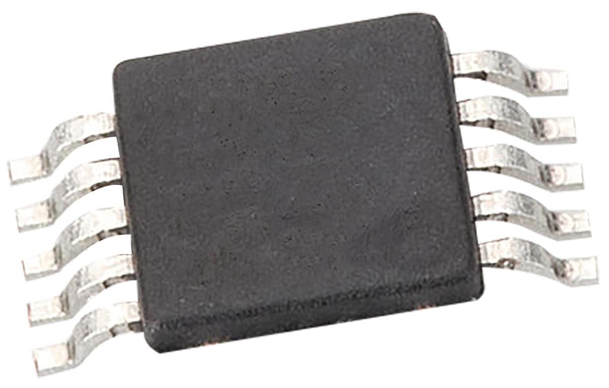
Package Type: DFN
Number of Elements per Chip: 1
Maximum Continuous Drain Current: 313 A
Pin Count: 8
FET Feature: –
HTSUS: 8541.29.0095
RoHS Status: ROHS3 Compliant
Operating Temperature: -55°C ~ 175°C (TJ) Package / Case: 8-PowerVDFN Rds On (Max) @ Id, Vgs: 0.87mOhm @ 50A, 10V Gate Charge (Qg) (Max) @ Vgs: 86 nC @ 10 V Vgs(th) (Max) @ Id: 3.5V @ 250µA REACH Status: REACH Unaffected edacadModel: NVMFSC0D9N04C Models FET Type: N-Channel Drive Voltage (Max Rds On, Min Rds On): 10V edacadModelUrl: /en/models/10427650Package: Tape & Reel (TR) Drain to Source Voltage (Vdss): 40 V Vgs (Max): ±20V Moisture Sensitivity Level (MSL): 1 (Unlimited) Power Dissipation (Max): 4.1W (Ta), 166W (Tc) Input Capacitance (Ciss) (Max) @ Vds: 6100 pF @ 25 V Qualification: AEC-Q101 standardLeadTime: 11 Weeks Mounting Type: Surface Mount Grade: Automotive Series: – Supplier Device Package: 8-DFN (5×6.15) Current – Continuous Drain (Id) @ 25°C: 48.9A (Ta), 313A (Tc) Technology: MOSFET (Metal Oxide) Base Product Number: NVMFSC0 ECCN: EAR99
This ismanufactured by onsemi. The manufacturer part number is NVMFSC0D9N04C. It has a maximum of 40 v drain source voltage. The product is available in surface mount configuration. The product carries enhancement channel mode. It provides up to 0.00087 ω maximum drain source resistance. The product carries 3.5v of maximum gate threshold voltage. The package is a sort of dfn. It consists of 1 elements per chip. While 313 a of maximum continuous drain current. It contains 8 pins. It is assigned with possible HTSUS value of 8541.29.0095. The product is rohs3 compliant. The product has -55°c ~ 175°c (tj) operating temperature range. Moreover, the product comes in 8-powervdfn. It has a maximum Rds On and voltage of 0.87mohm @ 50a, 10v. The maximum gate charge and given voltages include 86 nc @ 10 v. The typical Vgs (th) (max) of the product is 3.5v @ 250µa. In addition, it is reach unaffected. It carries FET type n-channel. The drive voltage (maximum and minimum Rds On) of the product includes 10v. It is shipped in tape & reel (tr) package . The product has a 40 v drain to source voltage. The maximum Vgs rate is ±20v. Its typical moisture sensitivity level is 1 (unlimited). The product carries maximum power dissipation 4.1w (ta), 166w (tc). The product’s input capacitance at maximum includes 6100 pf @ 25 v. It has a long 11 weeks standard lead time. The product is automotive, a grade of class. 8-dfn (5×6.15) is the supplier device package value. The continuous current drain at 25°C is 48.9a (ta), 313a (tc). This product use mosfet (metal oxide) technology. Moreover, it corresponds to nvmfsc0, a base product number of the product. The product is designated with the ear99 code number.
Reviews
There are no reviews yet.